![]()
![]()
- / Physical Design Course
Physical Design Course
Transform Digital Designs into High-performance Silicon with Precision
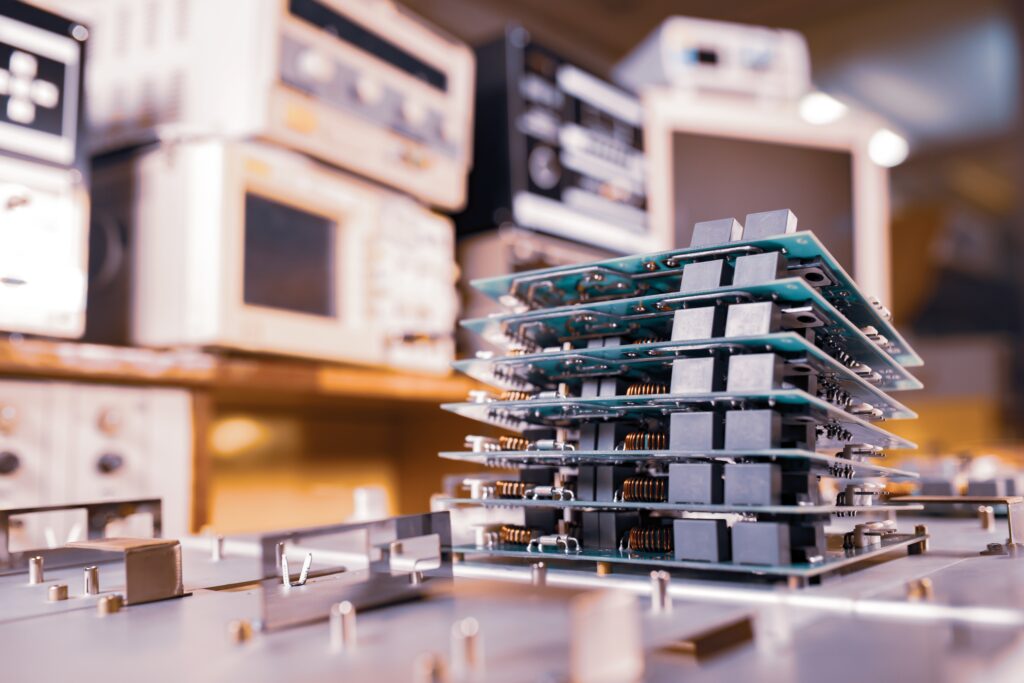
Physical design is a critical phase in the semiconductor development lifecycle, where digital logic is transformed into manufacturable silicon. Decisions made at this stage directly impact performance, power efficiency, and chip reliability.
KT Semicon’s VLSI Physical Design training course is crafted to develop industry-ready professionals who understand how to implement and optimise digital circuits at the physical level. This course delivers in-depth, hands-on training aligned with real semiconductor workflows.
Learners gain practical exposure to physical implementation stages used in leading chip design organisations. The focus remains on accuracy, optimisation, and timing closure, which are essential for building high-performance semiconductor devices.
Why Physical Design Skills Are Crucial In Semiconductor Engineering?
As semiconductor technology scales, physical design complexity continues to increase. Advanced nodes demand precise control over placement, routing, and timing to achieve performance goals. Even minor inefficiencies at the physical level can lead to higher power consumption or reduced yield.
This course addresses these challenges by developing a strong understanding of physical design constraints and methodologies. Our VLSI Physical Design training helps to gain clarity on how logical design choices translate into physical structures on silicon.

What Does This Course Cover?
The curriculum is structured to reflect industry-standard physical design flows. Each module of our physical design course builds practical competence while reinforcing theoretical understanding.
Floor Planning And Design Planning
Learners begin with floor planning, where the chip layout strategy is defined. This module covers block placement, power planning, and area optimisation techniques.
Participants understand how early design decisions influence timing, congestion, and power distribution. Strong floor planning skills form the foundation for successful physical implementation.
Placement & Optimization
Placement determines how standard cells are arranged on silicon. This module focuses on placement strategies that balance timing, power, and area.
Learners of the physical design course explore optimisation techniques to reduce congestion and improve signal integrity. Hands-on exercises help participants understand trade-offs involved in real designs.
Routing And Signal Integrity
Routing connects all design elements while meeting strict design rules. Learners work with global and detailed routing concepts, addressing challenges such as congestion, crosstalk, and routing constraints. The module emphasises clean routing practices that support reliable manufacturing.
Timing Analysis And Closure
Timing analysis is essential to ensure correct chip operation. This module introduces static timing analysis concepts, constraint management, and timing closure techniques.
Learners understand how to identify critical paths and apply fixes systematically. This knowledge is crucial for meeting performance targets in complex chips.
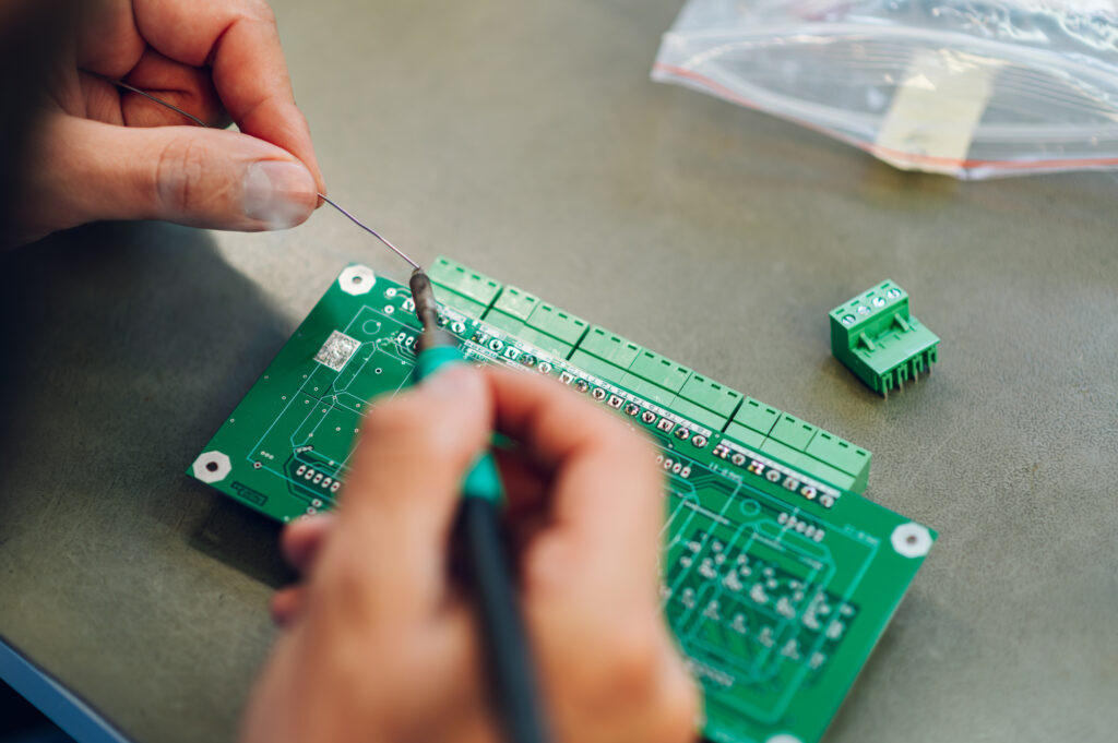
Practical Training with Industry-Relevant Workflows
KT Semicon emphasises hands-on learning throughout the program. Learners actively work through physical design stages using structured exercises and real-world scenarios. Each concept is reinforced through implementation tasks and analysis-based learning.
This approach helps learners understand not just how tools work, but why specific decisions matter. By the end of the VLSI Physical Design training, participants can confidently navigate physical design challenges and contribute effectively to semiconductor projects.

Career Opportunities after Course Completion
This course prepares learners for a range of core hardware engineering roles. The skills gained align closely with industry requirements across multiple sectors.
Common career paths include Hardware Design Engineer, PCB Layout Engineer, Hardware Test Engineer, and Hardware Integration Specialist. These roles are in demand across defence, industrial electronics, and technology-driven organisations.
Who Should Enrol in This Course?
This Hardware Design And Development course is designed for individuals who want to build or strengthen expertise in hardware design and development:
- Engineering Graduates: Ideal for those seeking a strong foundation in practical hardware engineering.
- Electronics & Electrical Engineers: Suitable for professionals aiming to enhance schematic and PCB design skills.
- Working Professionals: Beneficial for engineers involved in testing, integration, or system validation.
- Career Transitioners: Helpful for professionals moving into hardware-focused roles.
- Learners with Basic Electronics Knowledge: A foundational understanding of electronics supports effective learning.
Why Choose KT Semicon?
KT Semicon delivers training aligned with real semiconductor industry practices. VLSI Physical Design training is designed by professionals with hands-on experience in chip design and implementation.
Learners benefit from structured instruction, practical exposure, and career-focused guidance.