![]()
Understanding FPGA Internal Architecture: A Complete Beginner to Advanced Guide (2026)
Introduction
Field Programmable Gate Arrays (FPGAs) are one of the most powerful technologies in modern digital design. Unlike traditional processors or ASICs, an FPGA allows engineers to design custom hardware that can be reprogrammed at any time.
In this blog, we will explore FPGA internal architecture from beginner to advanced level, covering concepts like LUTs, CLBs, routing, and design flow in a simple and practical way.
What is an FPGA?
An FPGA (Field Programmable Gate Array) is a semiconductor device that can be configured after manufacturing to perform specific digital functions.
Unlike CPUs that execute instructions sequentially, an FPGA creates hardware circuits based on your design.
Key Idea:
FPGA doesn’t run software — it becomes hardware.
Why FPGA is Important
- Parallel processing capability
- Reprogrammable hardware
- High performance for real-time systems
- Widely used in VLSI, AI, and embedded systems
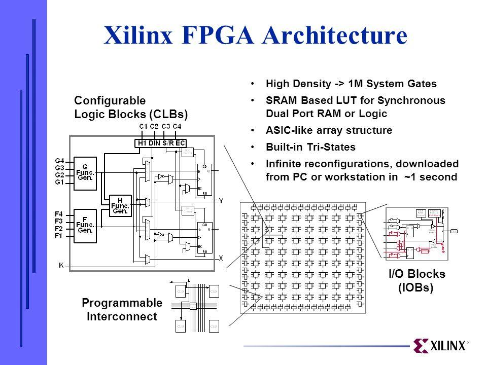
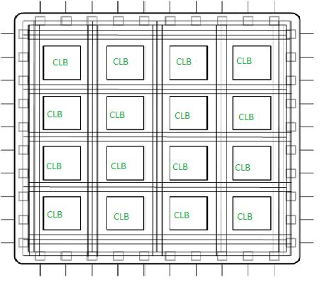
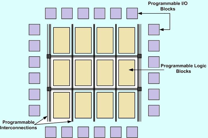
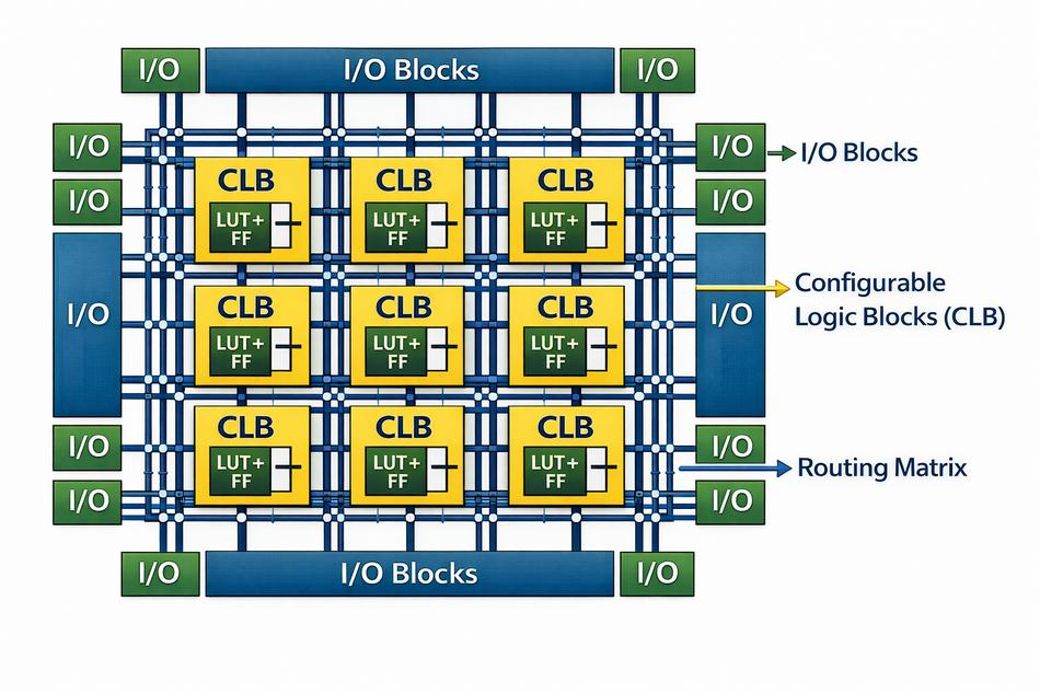
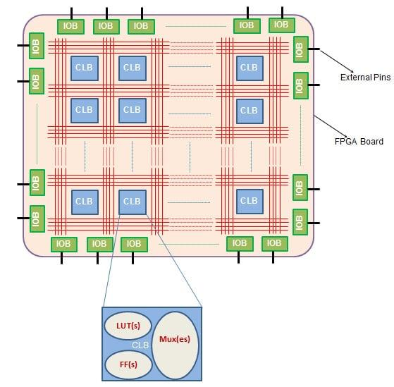
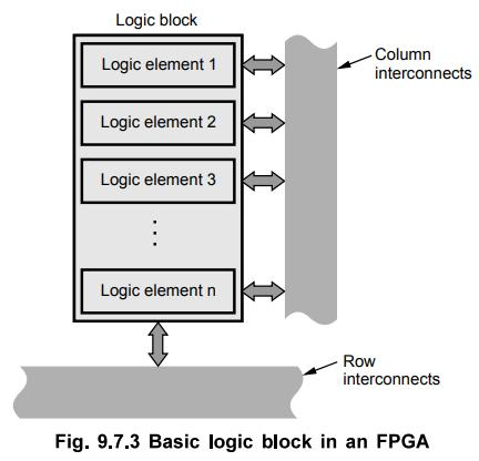
FPGA Architecture Overview
An FPGA consists of three major components:
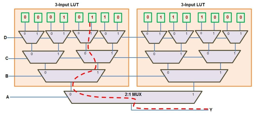
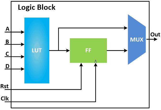
1. Logic Blocks (CLBs)
These blocks perform computations and contain LUTs and flip-flops.
2. Programmable Interconnects
These define how logic blocks are connected.
3. I/O Blocks
These connect FPGA to external devices.
FPGA is essentially a grid of configurable logic blocks connected via programmable routing.
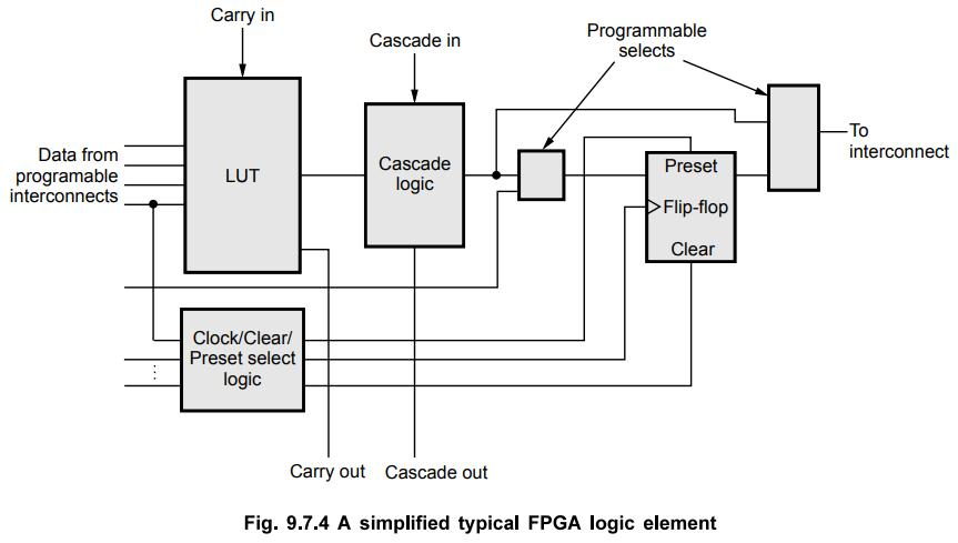
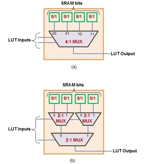
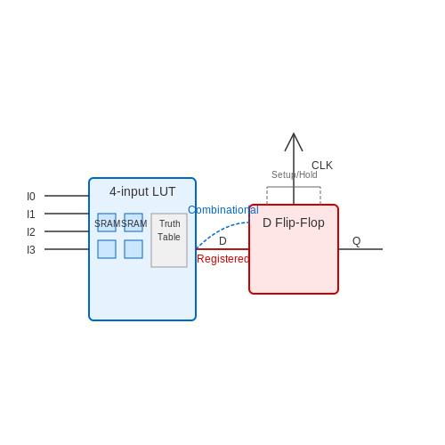
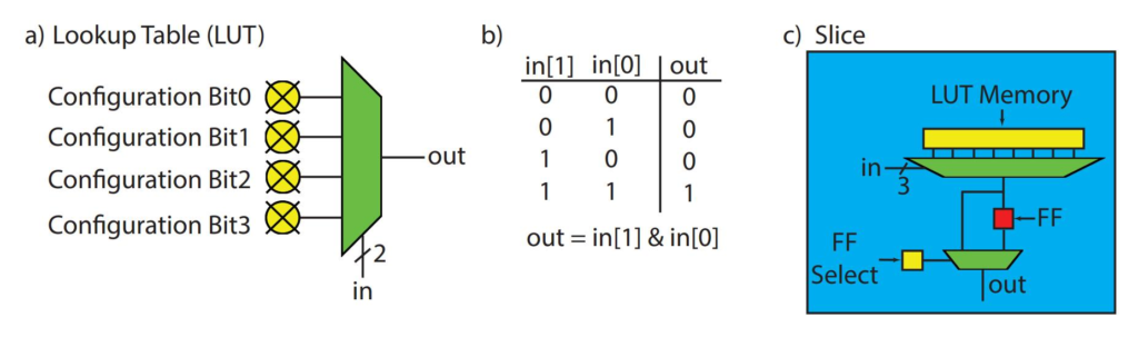
What is LUT in FPGA?
A Look-Up Table (LUT) is the fundamental building block of FPGA logic.
It is a small memory that stores output values for all possible input combinations.
Example:
For a 2-input LUT:
| A | B | Output |
| 0 | 0 | 1 |
| 0 | 1 | 0 |
| 1 | 0 | 0 |
| 1 | 1 | 1 |
Instead of calculating logic, FPGA stores the result in memory.
Key Concept
A LUT is not a logic gate — it is memory implementing logic.
This is the most important concept to understand FPGA architecture.
How FPGA Implements Logic
When you write a Verilog or VHDL code:
- The design is converted into logic equations
- Logic is mapped into LUTs
- Routing connects different blocks
- FPGA is configured using a bitstream
Final result: Your code becomes actual hardware.
FPGA Design Flow
- RTL Design (Verilog/VHDL)
- Synthesis (Convert to logic)
- Place and Route
- Bitstream Generation
- FPGA Configuration
Configurable Logic Blocks (CLBs)
CLBs are the core units of FPGA and include:
- LUTs for combinational logic
- Flip-flops for sequential logic
- Multiplexers
- Carry chains
These enable implementation of complex digital circuits like counters, ALUs, and state machines.
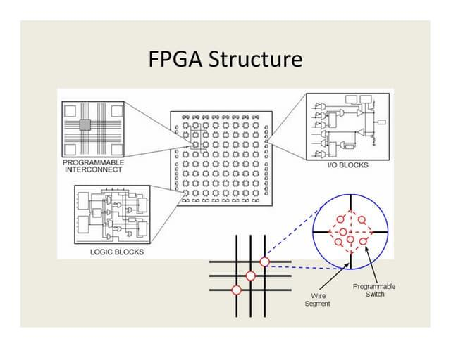
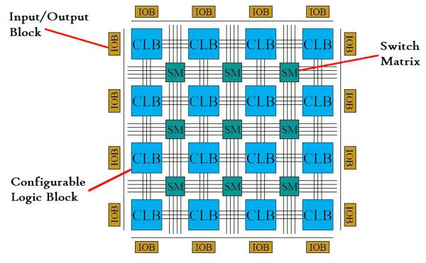
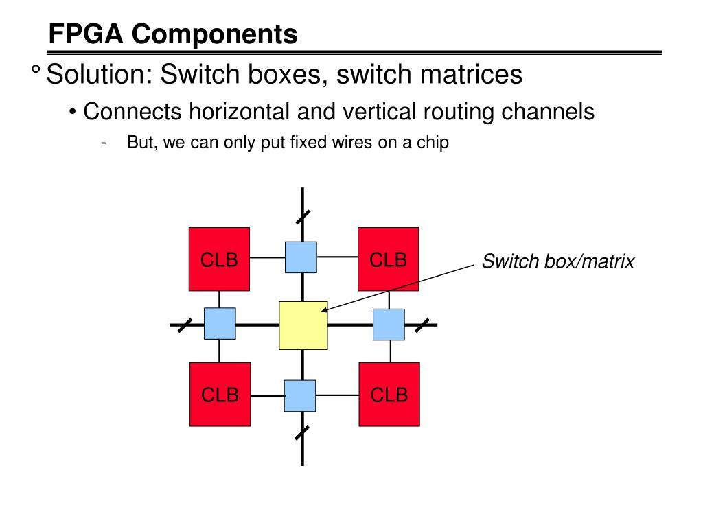
FPGA Routing Architecture
Routing is responsible for connecting logic blocks.
It includes:
- Switch matrices
- Programmable wires
- Routing channels
Routing directly impacts performance and timing.
Timing Concepts in FPGA
Important timing parameters include:
- Setup Time
- Hold Time
- Clock Delay
- Propagation Delay
Timing analysis ensures that the design works correctly at the desired clock frequency.
Routing: The Real Backbone
Routing decides:
- Signal delay
- Performance
- Timing closure
Even if logic is correct:
Poor routing = bad performance
Timing in FPGA (Critical for Advanced Level)
Key terms:
- Setup Time
- Hold Time
- Clock Skew
- Propagation Delay
Tools ensure your design meets timing constraints
Real Power of FPGA
Parallel Execution
- Multiple operations simultaneously
Custom Hardware
- Build your own processor / accelerator
Reconfigurability
- Update hardware anytime
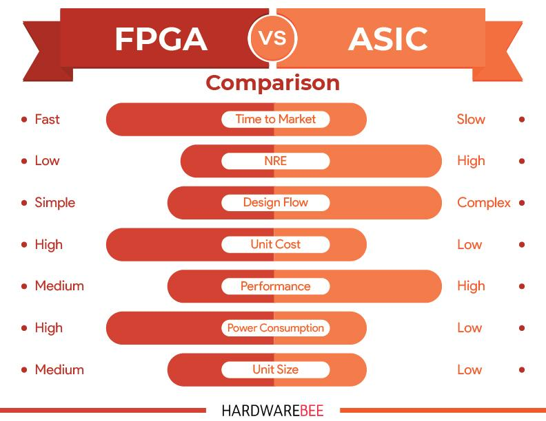
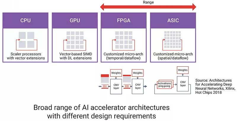
FPGA vs ASIC vs CPU
| Feature | FPGA | CPU | ASIC |
| Flexibility | High | Medium | None |
| Speed | High | Medium | Very High |
| Parallelism | High | Low | High |
| Cost | Medium | Low | Very High |
Applications of FPGA
- Artificial Intelligence
- 5G Communication
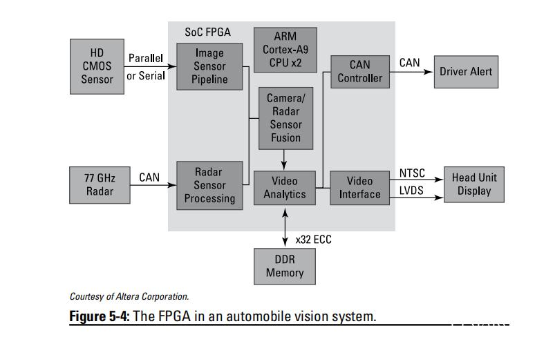
- Automotive Systems
- Cryptography
- Aerospace
Conclusion
FPGAs are powerful devices that allow designers to build custom hardware dynamically. By understanding LUTs, CLBs, and routing, you can unlock the full potential of FPGA-based design.
Final Thought:
FPGA doesn’t execute instructions — it rewires itself to become your circuit.